P. Giraud et al., Nanotechnology, 29, 7, 2018
Abstract
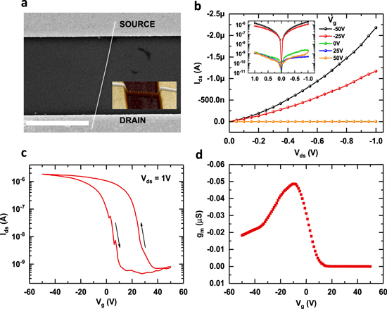
We demonstrate the fabrication of solution processed highly crystalline p-type PbS nanowires via the oriented attachment of nanoparticles. The analysis of single nanowire field effect transistor (FET) devices revealed a hole conduction behaviour with average mobilities greater than 30 cm2 V−1 s−1, which is an order of magnitude higher than that reported to date for p-type PbS colloidal nanowires. We have investigated the response of the FETs to near-infrared light excitation and show herein that the nanowires exhibited gate-dependent photo-conductivities, enabling us to tune the device performances. The responsivity was found to be greater than 104 A W−1 together with a detectivity of 1013 Jones, which benefits from a photogating effect occurring at negative gate voltages. These encouraging detection parameters are accompanied by relatively short switching times of 15 ms at positive gate voltages, resulting from a combination of the standard photoconduction and the high crystallinity of the nanowires. Collectively, these results indicate that solution-processed PbS nanowires are promising nanomaterials for infrared photodetectors as well as p-type nanowire FETs.